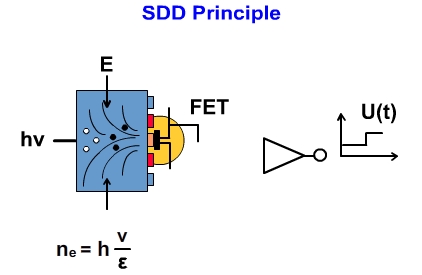
SDD Principle

The unique property of this type of detector is the extremely small value of the anode capacitance, which is independent of the active area. This feature allows to gain higher energy resolution at shorter shaping times compared to conventional photo diodes and Si(Li) detectors, recommending the SDD for high count rate applications.
To take the full advantage of the small output capacitance the front-end transistor of the amplifying electronics is integrated on the detector chip and connected to the collecting anode by a short metal strip. This way the stray capacitance of the interconnection detector - amplifier is minimized and moreover noise by electric pickup and microphony effects is insignificant. The anode is discharged from signal electrons in a continuous mode. Thus the SDD can be operated with dc-voltages only and there is no detector dead time caused by a clocked reset mechanism.
Due to the elaborated process technology used in the SDD fabrication the leakage current level is so low that the SDD can be operated with moderate cooling by means of a single stage Peltier element.
The SDD's energy resolution (FWHM < 145 eV @ MnKa, -20oC) can be compared to that of a Si(Li) detector requiring no expensive and inconvenient liquid nitrogen cooling. It surpasses the quality of pin-diodes.
To improve performance of the standard Silicon Drift Detector with regard to energy resolution and peak-to-background a new SDD-layout were developed. The integrated FET is no longer centered but moved to the outside margin of the structure. If a proper collimator is used, the FET is not irradiated by incoming photons.